I made a keyboard
#circuit-boards #keyboard #terrible-electrical-engineering
What have you made for yourself?
The Lobsters Blog Carnival started recently[1], with a deadline of 2025 September 17th. I may have… slightly missed that deadline in publishing this post.
The main topic was What have you made for yourself?, and in that spirit I’m choosing to make a keyboard from scratch in about three weeks (give or take about three weeks).
Layout
I’ve wanted to make a split (two separate halves that can be moved independently) columnar (where instead of staggering each row to the next, each column is staggered to the next) keyboard for a long time now. To begin with, I sketched the keyboard layout in Inkscape. To get a feel for the real scale, I changed Preferences → Interface → Zoom correction factor until it matched a ruler (read: smartphone) I held up to my screen.
Keeping it on-grid was annoying on a 1mm grid because I had to move by exactly 19 marks away each time. To make it easier, I changed to a 1.9mm grid to reduce this distance to 10 marks.
With the scale matched to real life, I could almost pretend to press keys directly on my screen to validate the layout.
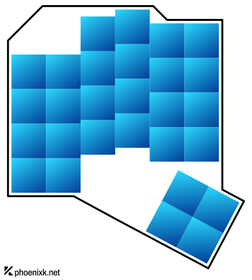
At this stage, I decided I’d use the same board for both halves by making the keyswitch footprint reversible.
Also, I had wanted to make a capacitive keyboard knowing nothing about capacitors or touchscreens. I’d probably need analog inputs to make capacitive sensors, but the nice!nano only breaks out two (or three depending on which pinout diagram you believe) analog GPIO pins of the nRF52840’s eight. Later, after I had ordered the circuit boards, I did a mild amount of clandestine measurement and found that the nice!nano uses a 7x7mm nRF52840 package—that’s the aQFN73 package, which I would not be able to solder jumpers to owing to it being a ball grid array with no exposed pads whatsoever. It doesn’t expose any pins to the outside!
I had been hoping it was using the QFN48 package, which exposes pins somewhat to the outside. (Fun curiosity: because it has 48 instead of 73 pins it can be a full millimeter smaller on each side, measuring 6x6mm.)
My plan was to leave the board dual-purpose: to make it capacitive I would have cut the traces for rows 1-3 and wired jumpers from there to analog pins on the nRF52840, leaving the other rows as regular key switches. As a micro-optimization (foreshadowing!), I put solder bridges here so that instead of cutting if need be, I’d only have to put a blob of solder on each one to jumper each trace to its respective digital pin.
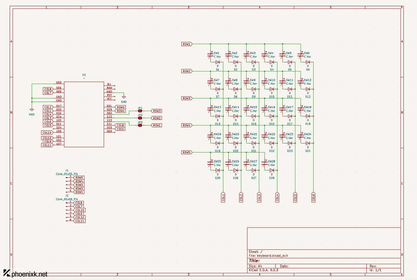
With the schematic in hand, I could start to lay out the same circuit board that I’d use for both sides. One cool trick here is that I laid out the column-to-column traces in columns and then placed every other column on the front side of the board, leaving room for the row-to-row traces to travel all the way across the board uninterrupted.
Another unconventional trick (as far as I can tell, and I didn’t look too far!) was that I routed all the traces out to a grid of diodes, and then back to the MCU. This meant I could expend much less mental effort when I would later have to turn into a human pick-and-place machine.
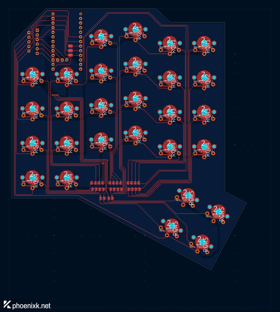
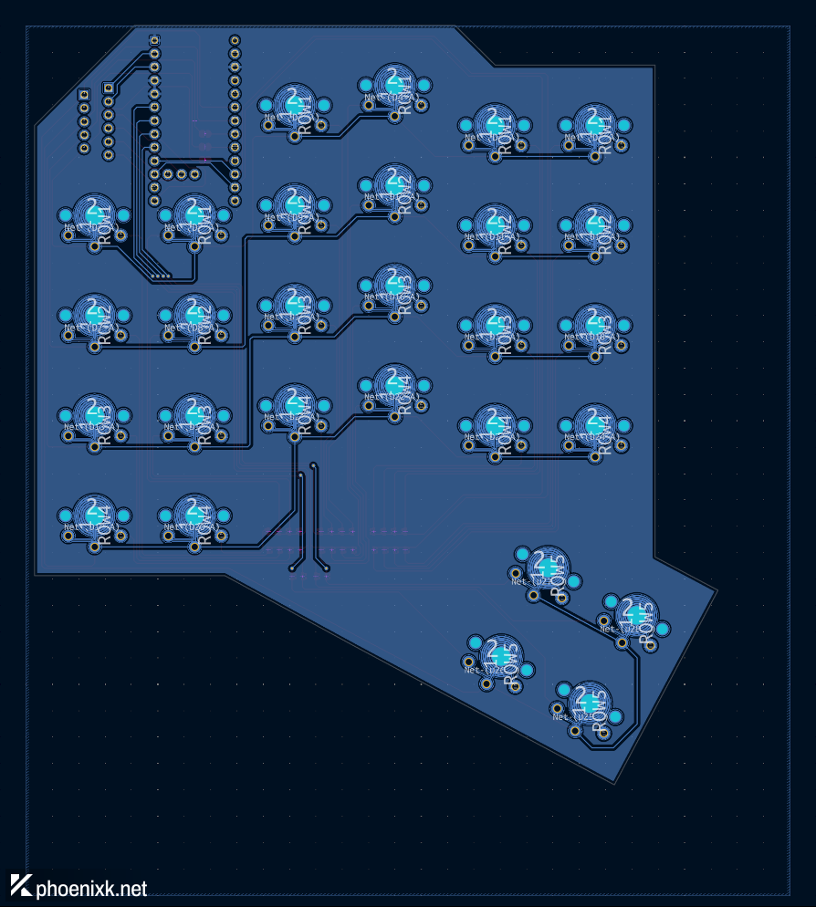
It took a day or so and three attempts to lay out the circuit board until I got to something I was happy with. (Astute readers may note that there’s no way to attach miscellaneous auxiliary objects to this board, such as feet or a case.)
Assembly
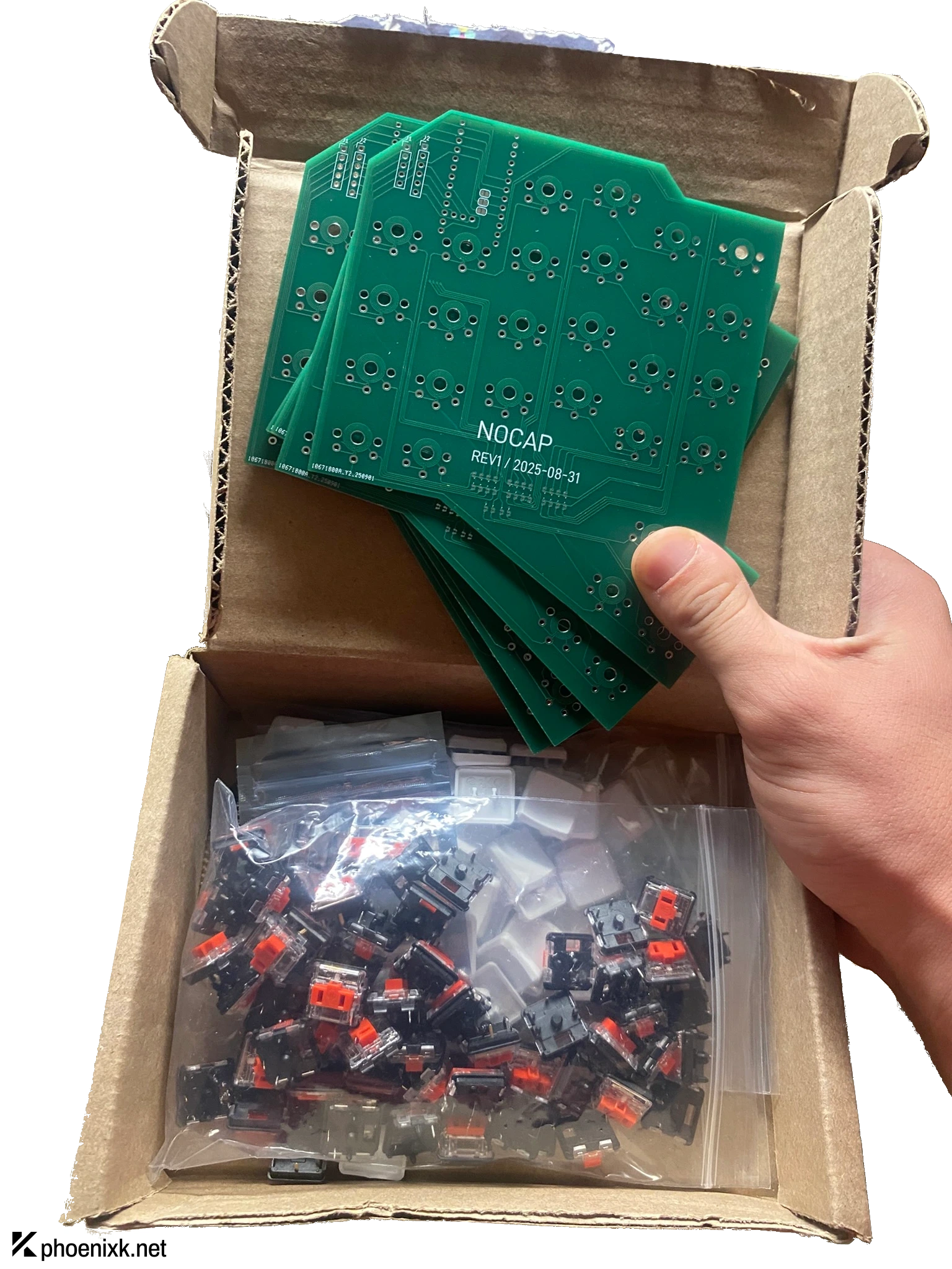
Two weeks later, all of the parts I’d ordered had arrived. Not pictured: the stencil. Yeah, I forgot to order this with the boards themselves, and when I did order them I didn’t notice an option to order a reasonably-sized stencil. I did notice the box that the stencil arrived in, which was about 300 by 300 millimeters.
Applying solder mask is pretty easy; you line up the stencil to the board and then use a scraper to push as much solder paste as you can through the stencil’s holes and onto the exposed pads.
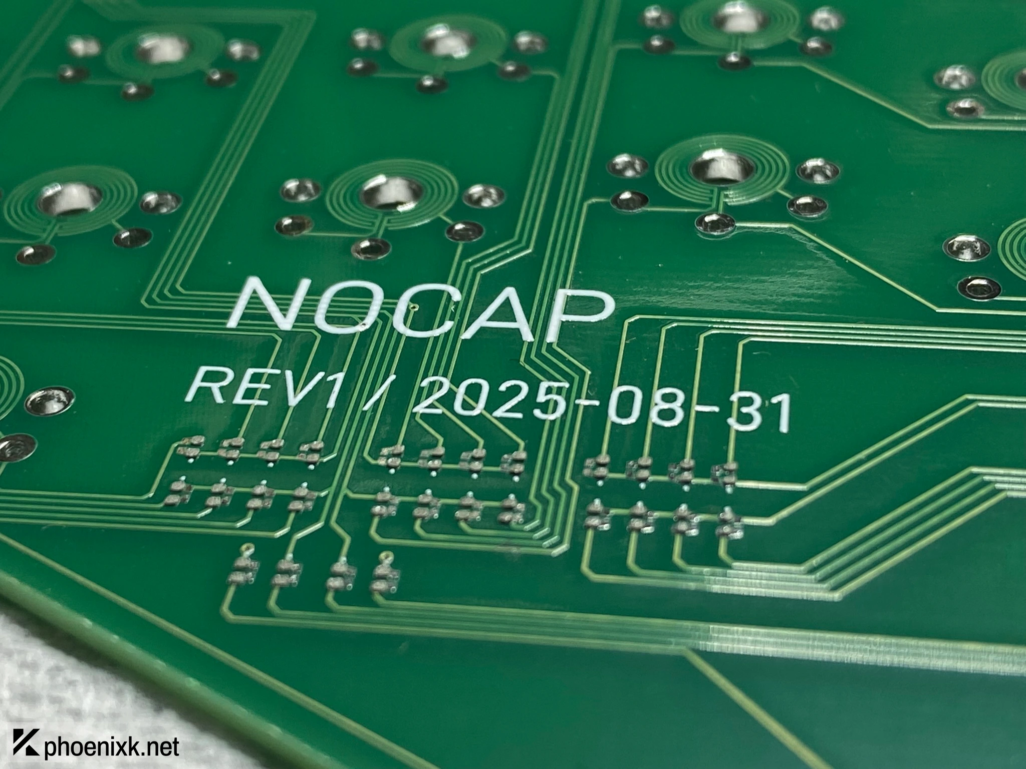
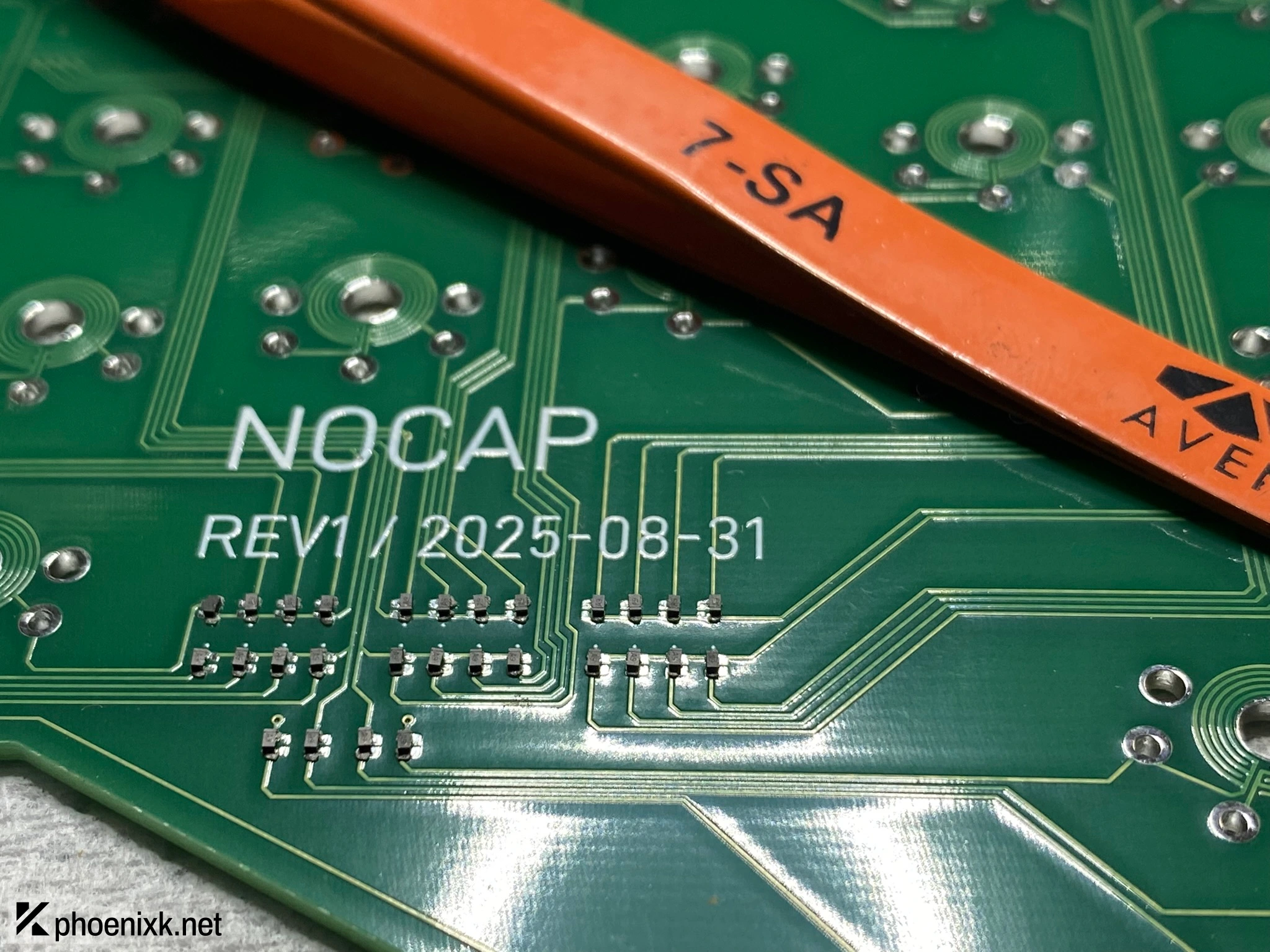
After I put all the diodes on, fifteen minutes in the oven[2] flowed the solder nicely. I had put on a little too much solder paste here—instead of lying flat, the solder had balled up enough that the diodes could fall to one side. Next time I’d definitely pull the solder stencil back a bit in KiCad.
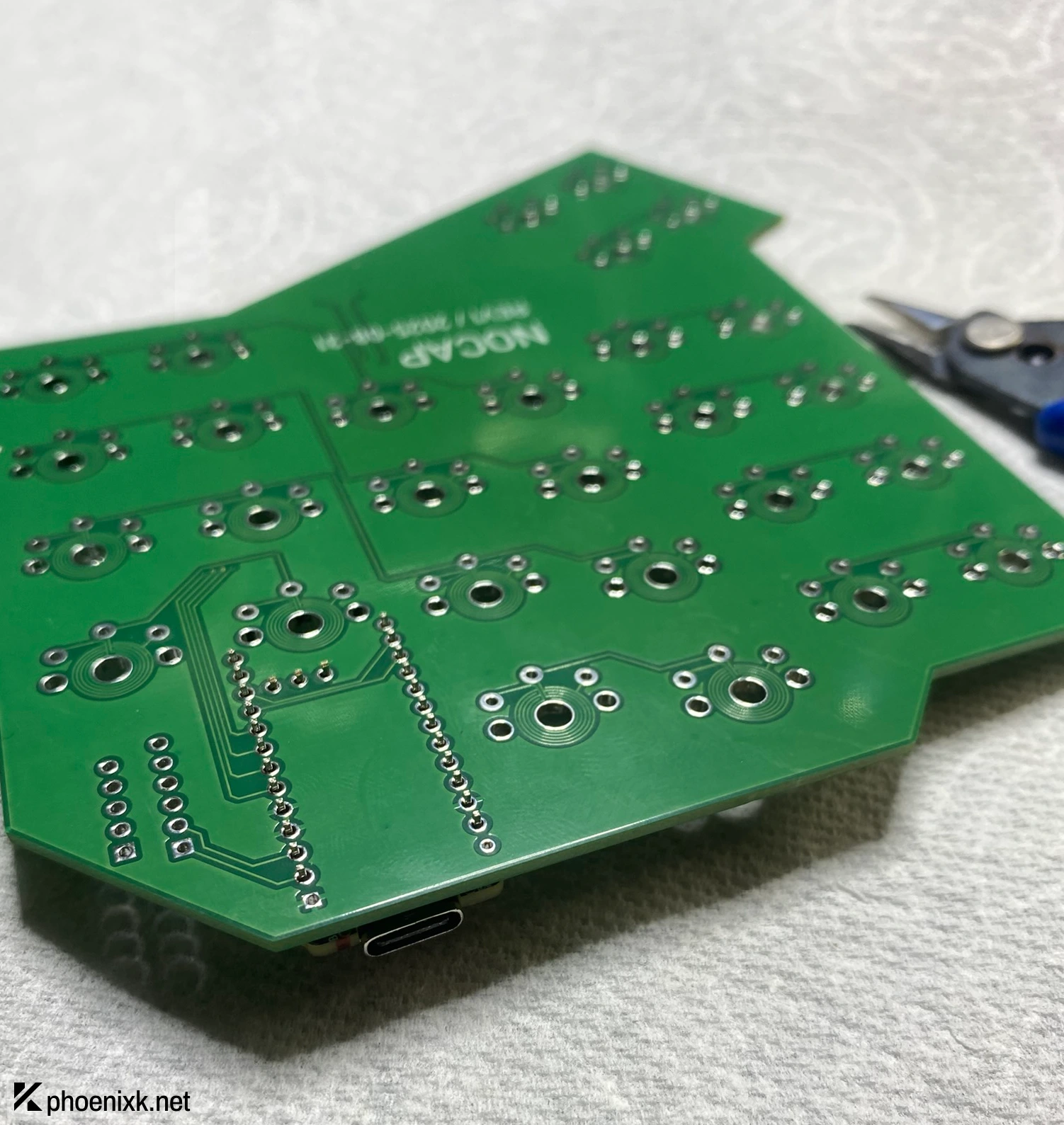
Using two processors for a single keyboard had always seemed a waste[3], so I’d always intended to put the entire passive half’s matrix over the cable. Each half of my keyboard is a 6x5 matrix, so I’d need eleven conductors. You know what has eleven conductors? USB-C cables. Not Ethernet. Ethernet cables have eight conductors. Eight conductors is not enough—
So here’s a twisted-pair-twisted-pair dual-Ethernet cable.
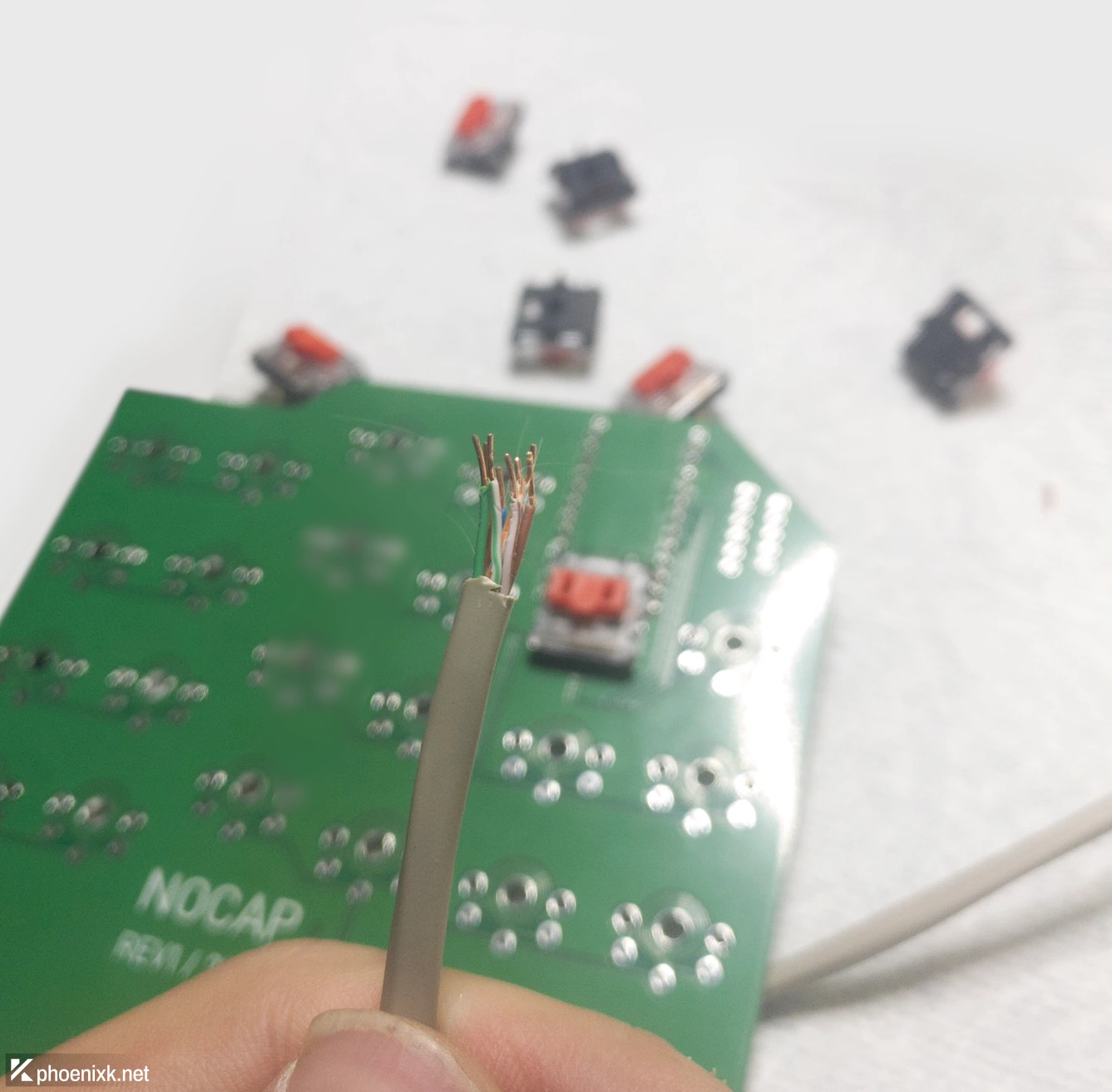
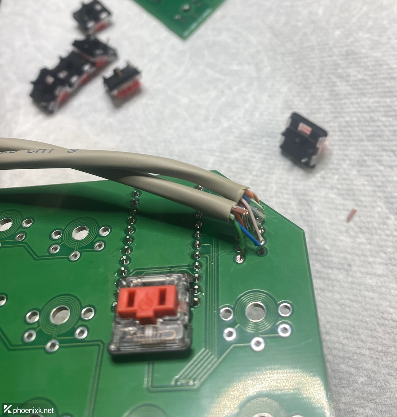
It was here that I’d realised I never soldered the solder bridges together, leaving rows 1 through 3 disconnected! And now that I’d soldered on the microprocessor, I couldn’t get access to the solder pads that were under it. And I wasn’t about to de-solder 23 header pins; that would hurt a lot. Instead I just soldered a few jumpers.
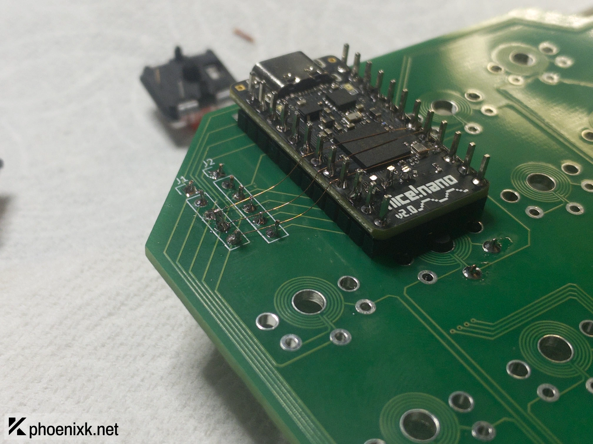
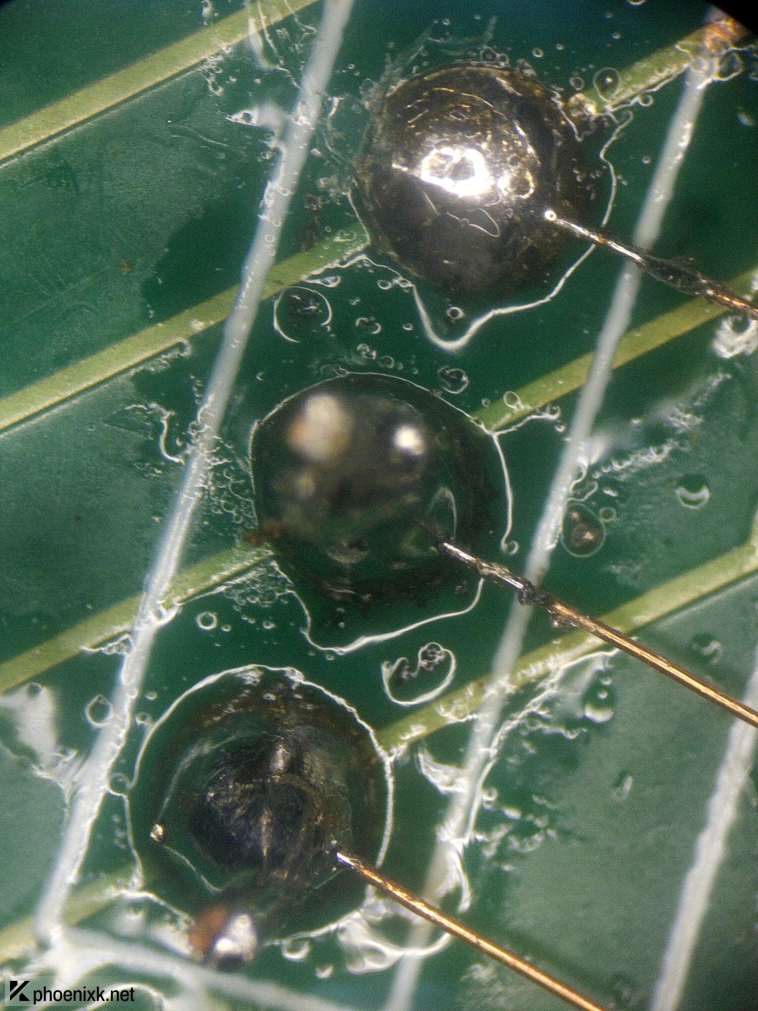
I didn’t take any pictures of me assembling the other side of the keyboard, so you’ll have to imagine much the same again.
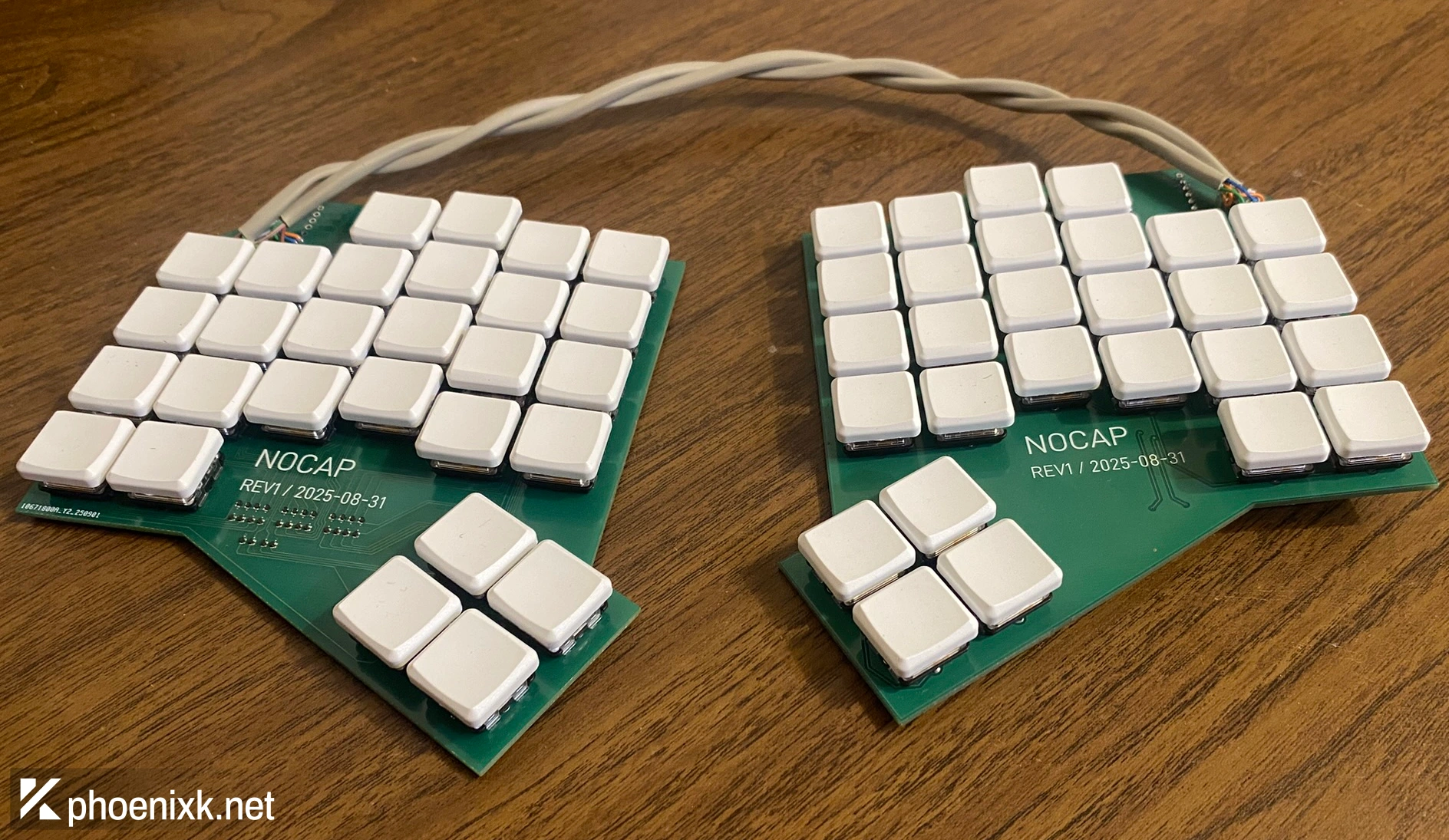
..and there it is! A keyboard!
Software
The nice!nano is A Microprocessor For Bluetooth Keyboards, which has consequences.
QMK (what seems to be the going standard for keyboard software) doesn’t work on the nRF processor. Nice Technologies LLC recommends either ZMK or BlueMicro. After half an hour and 3 gigabytes of Git repositories (how is a keyboard going to need half of Linux I’ll never know), I switched to BlueMicro in a fit of anger.
For a time, the left half still had ghosting.[4] This was probably because of the long cable across, which could have had electrical crosstalk and/or industrial levels of capacitance. (again: not an electrical engineer.)
I fixed this by bumping up the scan delay a bit, then shortening the cable, then reducing the scan delay back to what it was.
I also ran into a problem where the keyboard kept rebooting, although it could’ve been simply disconnecting from USB? After a few false starts and judicious use of the “comment out region” key in my editor, I narrowed it down to the Bluetooth connection.
Removing this seemed to fix it, by adding keyboardconfig.connectionMode = CONNECTION_MODE_AUTOCONNECTION_MODE_USB_ONLY
to setupConfig. Apparently connecting to Bluetooth meant disconnecting from USB? I’m not sure, it’s been a while.
Simply not supporting Bluetooth was fine for me, as my keyboard doesn’t even have a battery. Even then, though, it still kept rebooting after about 30 seconds of inactivity. It turns out, what I had to do was…
Matrix Debugger Interlude
Each board has four columns of header pin sockets: two for the nice!nano, one for ROW1-5 to solder to, and finally one for COL7-12, where I’d solder a cable across to the passive half’s COL1-6.
I initially wired COL1 through COL4 on the left side of the nice!nano header socket, and COL5 and COL6 on the right side. But then I realized that to connect the two halves, it’d be nice to have six consecutive pins in a row to solder to, instead of jumping from one side to the other.
So I moved COL5 and COL6 to the left side instead. Because the traces next to the nice!nano had already morphed into a space-filling curve, the easiest way to lay these traces was to use a via to flip to the other side of the board.
You know what a via is? A hole through the board.
You know what a header pin socket is? A hole through the board.
Using the header pin sockets as vias I could route COL5 and COL6 to the same side of the nice!nano as COL1 through COL4. As a downside, this meant that these two columns were wired to two different GPIO pins each. This shouldn’t break anything, riiight?
Connecting a single column to two different GPIO pins breaks BlueMicro’s GPIO matrix debugger.
Here’s how to cut a trace on a circuit board:
- Hope and/or guess it’s a two-layer board
- Stab the board with a knife
Mysteriously, the debugger works now! The extra traces were only useful on the passive half, so I didn’t even have to jumper them back together.
Giving my keyboard insomnia
Linux will let USB connections go to sleep immediately. “Going to sleep” here means it’s sending a “please stop doing anything” packet over USB.
And it appears that BlueMicro interprets “please stop doing anything” to mean “disconnect from USB after 30 seconds”. This confused me for a while because it shows up exactly the same way as the Bluetooth issue.
Thankfully, there’s a builtin #define that will simply ignore Linux. After toggling that flag…
//#define SLEEP_ACTIVE 1
#define SLEEP_ACTIVE 0
it worked perfectly!
Takeaways
It’s really annoying that the active half sits much taller than the passive half, owing to the microprocessor sticking out half an inch and the feet being “whichever header pins are on the convex hull”. A case would really help me out.
The ethernet cable’s solder joints have broken several times already, and I’ve barely used this keyboard for perhaps a hundred letters. It hurts, but next time I’d skip the hassle, make it battery operated, and actually use it more than three times ever. Heck, next time may be the time I skip the breakout board and put a processor right on my own board! (See you in the late 2030s!)
Also, even though my pinky finger did rest that far off from the rest of the keyboard on the screen, that did not transfer over to the keyboard proper at all. The two pinky rows were wildly out of reach and I kept losing track and drifting up a row on those two columns. In the future, I would definitely just keep the same middle-to-ring-finger offset for the ring-to-pinky offset.
Bonus: any data is a shell script if you use enough editor macros
Reveal at your own risk.
#! /usr/bin/env sh

rm watermarked/*

IMAGE() {
	,mark _edited/$2.png $3 $4
	ffmpeg -y -i _edited/$2.watermarked.png -quality 93 watermarked/$2.$1
}

# extension, basename, watermark-style, watermark-dpi
IMAGE	png	schematic	light	36

IMAGE	png	board-f-cu	dark	36
IMAGE	png	board-b-cu	dark	36

IMAGE	png	diode-footprint-detail	dark	36

IMAGE	webp	parts	light	42

IMAGE	webp	solder-mask-applied	light	60

IMAGE	webp	diodes-placed-6x	light	60
IMAGE	webp	diodes-placed-all	light	60

IMAGE	webp	nice-nano-pre-solder	light	60

IMAGE	webp	ethernet-conductors	dark	60
IMAGE	webp	ethernet-soldered	dark	60

IMAGE	webp	jumpers-tiltshift	light	60
IMAGE	webp	jumpers-microscope	light	60

IMAGE	webp	finished	dark	80
-
I don’t want to talk about it.↩
-
It wasn’t a regular oven. Don’t use a regular oven.↩
-
You know what’s even more wasteful? Having an entire new keyboard you never use because of how bad it is.
Product market fit, everyone. Especially if the market is you.↩
-
It turns out there’s a reason most people don’t wire matrices together using Ethernet. Yes I know it’s not actually Ethernet that makes it worse.↩